Electric field probe calibration: key for accurate measurements
- Apr 14, 2021
- 6 min read
Updated: Aug 23, 2024
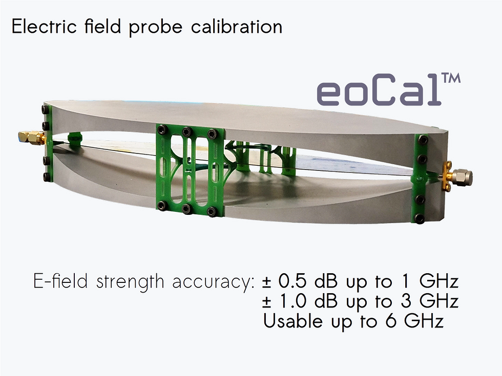
Kapteos is introducing a breakthrough for electric field probe calibration through an Adiabatic TEM cell (ATEM).

Electric (E)-field probes are of key interest for a wide range of applications: antenna testing, SAR measurement, MRI safety, EMC pre compliance, high voltage measurements, plasma plume dynamics, HPEM…
For most applications, an absolute value of the E-field strength needs to be assessed. Hence, electric field probe calibration is of key importance. For that purpose an E-field applicator generating a perfectly known E field both in direction and magnitude is required.
Major E-field applicators can be classified in three broad categories:
- plane-parallel capacitors for low frequency applications
- GTEM cells for high frequency applications
- TEM and Crawford cells for applications up to a few GHz
Plane-parallel capacitors are easy to produce but they need to be symmetrically powered (positive signal on one electrode while an opposite signal is delivered to the other electrode) and considerable care must be taken for the design of the electrodes in order to homogenize the E field in the gap between electrodes. If such design rules are not followed, large deviations (± 2 to ± 4 dB) could be observed between theory (applied voltage divided by gap width) and practice. Another drawback of this E-field applicator concerns its operating frequency range that is upper bounded in the MHz range.
On the contrary, GTEM cell theoretically doesn’t present any upper bound concerning their operating frequency range. However, the impedance loading of the GTEM cell remains tricky and their standing wave ratio is generally too high to get a well defined E field. E-field strength is usually known within an accuracy of ± 2 to ± 3 dB.
TEM cells and Crawford cells present the key advantage of being two port devices, thus allowing to measure both reflected (S11 parameter) and transmitted (S21 parameter) waves through the use of a Vector Network Analyzer (VNA). However, the abrupt transition between central and tapered sections of the TEM cell leads to a mode mismatch and then to the generation of higher order propagation modes. As a consequence, such cells present a quite low upper bound of their operating frequency range (typically 1 GHz or less).
Kapteos introduces here an innovative concept of ATEM cell that consists in removing the abrupt transition between central and tapered sections that is encountered in a classical TEM cell. Despite the size of this ATEM cell, this latter one exhibits no higher modes up to 6 GHz.
Once having an efficient E-field applicator 6 main issues have to be addressed before being able to carry out accurate electric field probe calibration.
1st issue: Standing wave
In order to illustrate the standing wave issue for electric field probe calibration, a CPW line with a mismatched impedance (80 Ω) has been loaded by 50 Ω and connected to VNA port 1. A near field electric field probe eoProbe™ has been connected to VNA port 2 as shown. Then an E-field map at DUT surface has been carried out, exhibiting nodes and anti-nodes at fixed positions along the Coplanar WaveGuide (CPW) line. Accuracy on E-field strength worsened rapidly with the increase of Voltage Standing Wave Ratio (VSWR). To keep an accuracy on E-field strength better than ± 0.5 dB, VSWR must be lower than 1.12 (S11 < -24.8 dB).
2nd issue: E-field enhancement near metallic parts
In order to illustrate the E-field enhancement issue, 2D ElectroMagnetic (EM) simulations have been carried out considering a 5.5-mm diameter near field electric field probe ET5-air placed between two parallel plates.
In case of a probe with a centered position between the two parallel plates, no significant E-field enhancement (i.e. no enhancement greater than 0.5 dB, i.e. 5.9%) occurs for an inter-electrode distance greater than 3 times the probe diameter. However, when the probe is clamped to one electrode, the E-field enhancement tends towards a low of 15%.
This E-field enhancement phenomenon originates from the Maxwell continuity equation at the interface between two media not presenting the same permittivity: it is growing with the increase of both permittivity mismatch and probe relative size.
In conclusion, the smaller the E-field probe and the lower its effective permittivity, the smaller is the measurement artifact induced by this E-field enhancement phenomenon. For that reason, Kapteos near field electric field probes are of different type (air and bio lines) in order to keep the permittivity mismatch with the measurement medium as low as possible. Moreover, for a distance of air line probes to nearest metallic element greater than 5 mm, the accuracy on E-field strength is kept better than ± 0.5 dB. This is the reason why Kapteos ATEM cell presents a septum to ground plane of 17.4 mm > 5.5 mm (probe diameter) + 2 x 5 mm.
3rd issue: Interference induced by the E-field probe
Another important issue, generally underestimated, concerns the interference induced by the E-field probe on the E-field distribution inside the E-field applicator. An easy and cost effective way to characterize the impact of the E-field probe presence inside the E-field applicator consists in measuring the transmitted RF power by the TEM cell versus the position of the E-field probe. For single port E-field applicators like GTEM cells, a slightly more expensive characterization bench is required: it is based on a VNA to measure the reflection (S11 parameter) of the injected RF power to the GTEM cell versus the position of the E-field probe.
As seen on the illustrations, measurable interference is neither induced at 100 MHz nor at 1 GHz, whatever be the near field electric field probe position inside the ATM cell. On the contrary, a periodic modulation of transmitted RF power appears at 10 GHz, exhibiting a periodicity of λ/2. At this latter frequency, high order modes are present in the ATEM cell and the probe introduces an extra boundary condition that is probe-position-dependent and that modifies the distribution of the TEM modes, each TEM mode presenting its own power transmission coefficient.
4th issue: Electromagnetic Interference in calibration bench
When making accurate calibration, a special care has to be considered concerning potential ElectroMagnetic Interference (EMI) in the calibration bench. It is of key importance to check that no EMI (conducted and radiated) contributes to the measured signals. Whereas it is easy to stop the emission of the RF source, there is no way to remotely power off the E field probe when a classical E-field probe, like a reference antenna, is used.
For that purpose, a 50 ohms has to be plugged in the RF cable instead of the reference antenna. However, in that case the EMI assessment is not carried out with the same experimental configuration than the one used for calibration procedure. With Kapteos near field electric field probe, you just need to switch off the laser source to remotely power off the E field probe while maintaining the system exactly in the same experimental configuration. EMI assessment is then straight forward as switching off the laser lets you know if you are concerned or not by EMI.

5th issue: RF link Insertion Loss
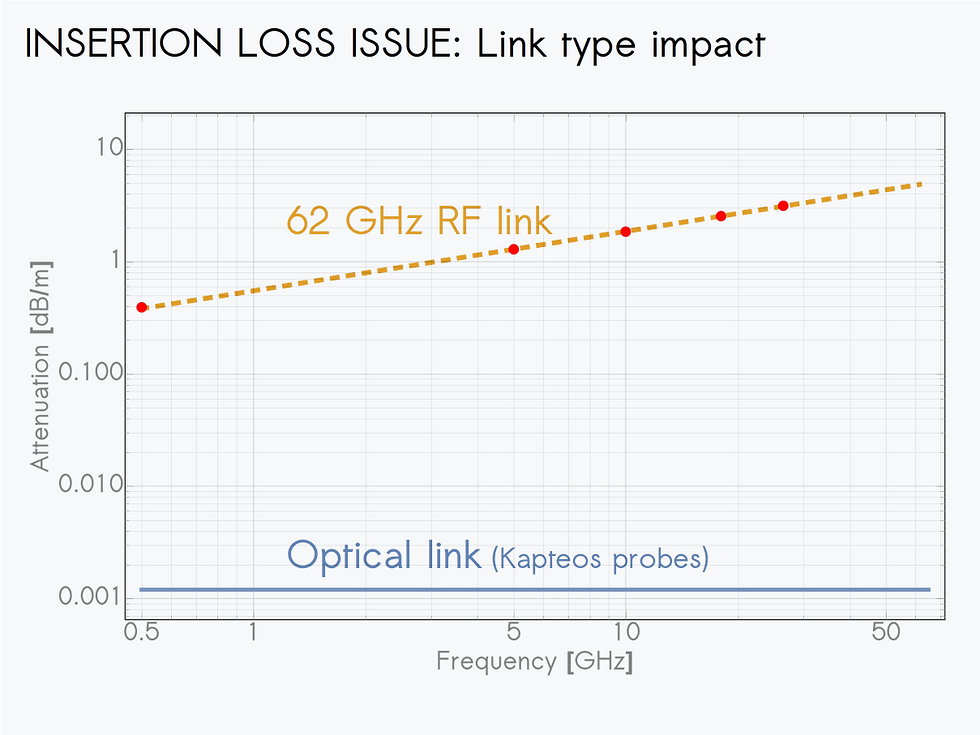
During electric field probe calibration the Insertion Loss (IL) of the physical link between the E-field probe and the signal digitizer has to be precisely assessed. With an E-field probe using a RF link, its IL is usually measured during the VNA calibration procedure by bringing the RF-link end back to VNA port 2. However, this requires to fold the RF cable which leads to a IL change (both in magnitude and phase). The longer is the RF link and the higher is the operating frequency, the higher is this effect.
With Kapteos near field electric field probe, IL is not an issue in practice. Indeed, as the IL is measured in real time, we get rid of IL changes while the probe is moving as it is possible to subtract in real time any IL change. Moreover, IL is lower than 0.0012 dB/m whatever the frequency of interest (DC to 100 GHz) whereas the it is higher than 5 dB/m for a RF cable link at 65 GHz.
6th issue: Signal-to-Noise Ratio
The Signal-to-Noise Ratio (SNR) is the last parameter limiting the accuracy of the electric field probe calibration. E-field probe SNR is easy to obtain via a measurement using a field applicator and an Automatic Spectrum Analyzer (ASA). This SNR gives the accuracy floor with which the electric field probe calibration can be carried out.
To get an accuracy on E-field strength better than ± 0.5 dB, SNR must be greater than 23 dB.
Electric field probe calibration with ATEM cell: setup for accurate measurements
The simple experimental setup illustrated here has allowed to address five out the six issues discussed above. The only one that has not been addressed by this setup concerns the main issue of measuring the SWR in the ATEM cell for which a VNA is required.
With use of ATEM cell Kapteos near field electric field probes are calibrated with an accuracy of ± 0.5 dB up to 1 GHz and with an accuracy of ± 1 dB from 1 to 3 GHz.
For more information, feel free to contact us.


Comments